3. SEM Signal Modes
Secondary Electrons · SE
Secondary electrons are low-energy electrons emitted from the first few nanometers of the sample surface. Because they originate so close to the surface, they are extremely sensitive to relief and topography. Edges, slopes, and protrusions emit more secondary electrons and therefore appear brighter in SE images.
SE imaging is the most common SEM mode and provides intuitive, three-dimensional renderings of surface texture in metals, ceramics, polymers, and biological specimens.
▸ Technical parameters
- Energy range: typically < 50 eV
- Escape depth: ~0.5–5 nm
- Detectors: Everhart-Thornley (ETD), in-lens (ILD)
- Resolution: highest of all SEM modes in FE-SEM
- Limitation: charging artifacts in non-conductive samples
- Low kV (1–5 kV) improves surface specificity and reduces charging
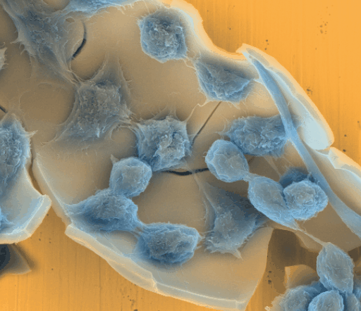
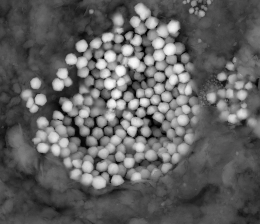
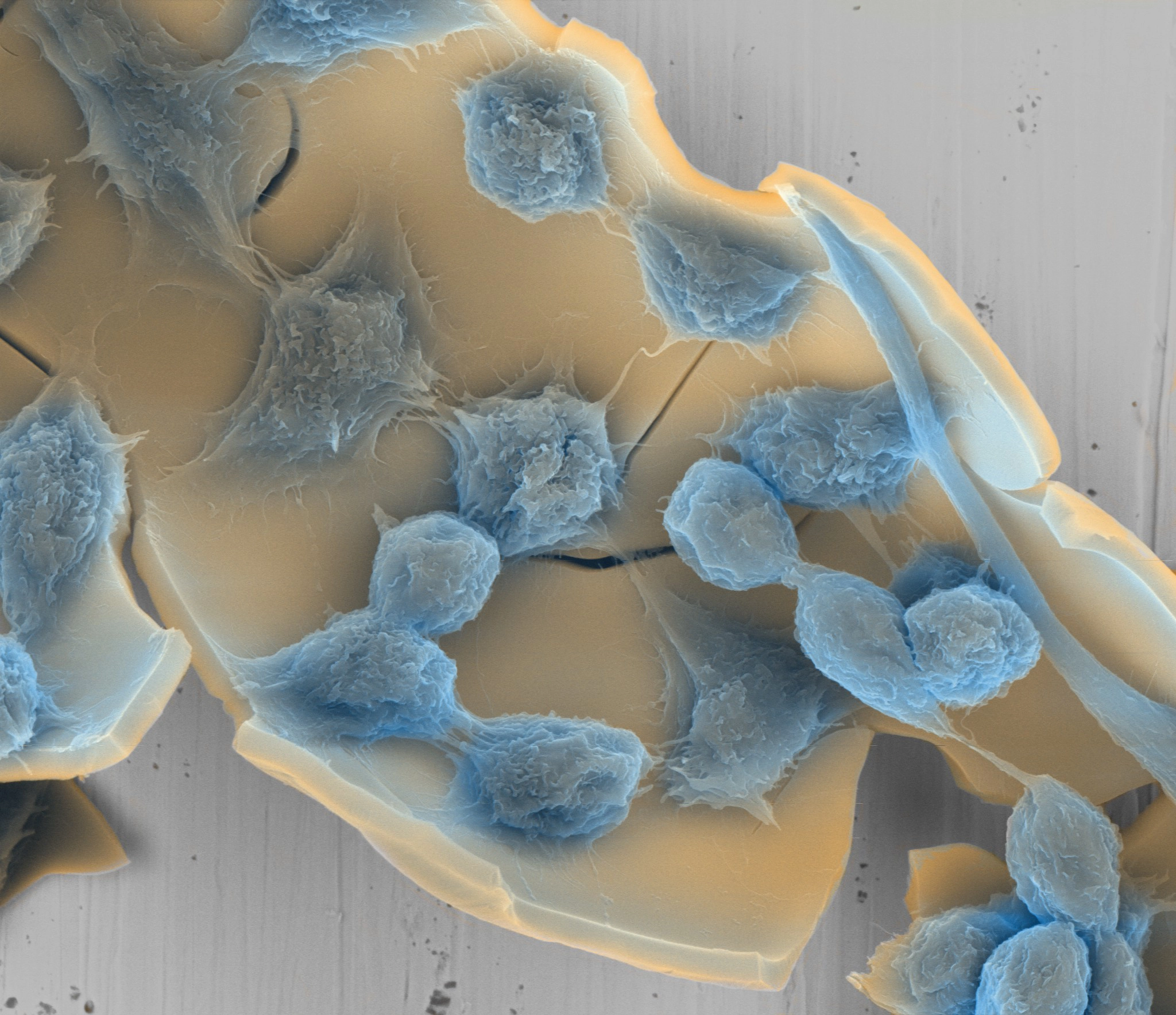 Cells on biocompatible ceramic surface · SE
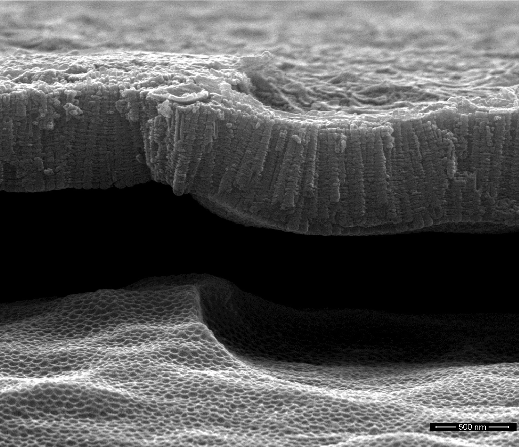
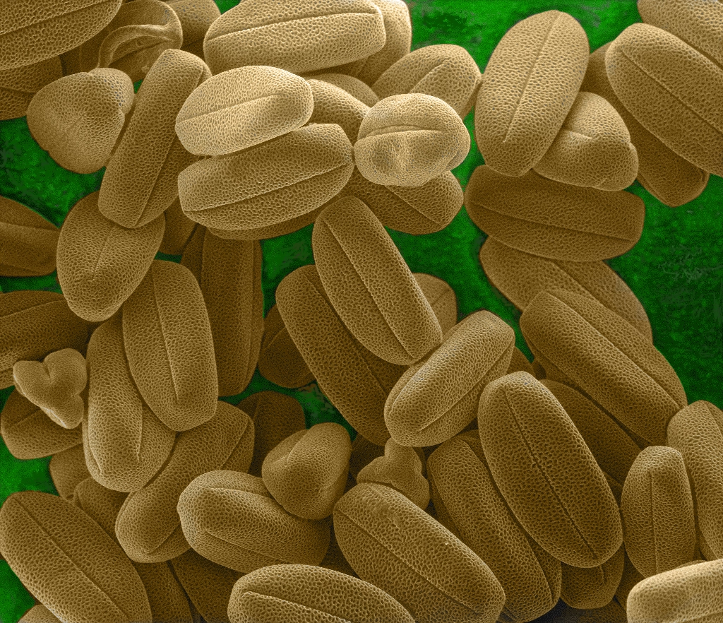 Pollen surface microstructure · SE
Backscattered Electrons · BSE
Backscattered electrons are primary beam electrons that have been deflected back out of the sample by elastic scattering. Heavier elements scatter electrons more strongly than lighter ones — regions containing elements of higher atomic number appear brighter in BSE images, providing direct compositional contrast.
BSE imaging is widely used in geology, metallurgy, and materials science to separate mineral phases, alloy components, or inclusions based on average atomic number, even when their surface topography is similar.
▸ Technical parameters
- Energy range: 0.2E₀ to ~0.9E₀ (high fraction of primary energy)
- Escape depth: larger than SE — ~100 nm to several μm depending on E₀ and Z
- Detectors: solid-state annular BSE detector above the sample
- Spatial resolution: lower than SE due to larger interaction volume
- Higher kV (10–20 kV) enhances atomic number contrast in BSE
- BSE coefficient η increases monotonically with atomic number Z
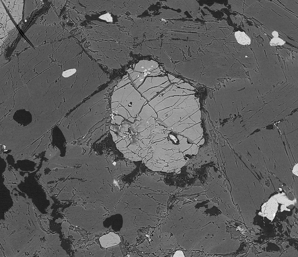
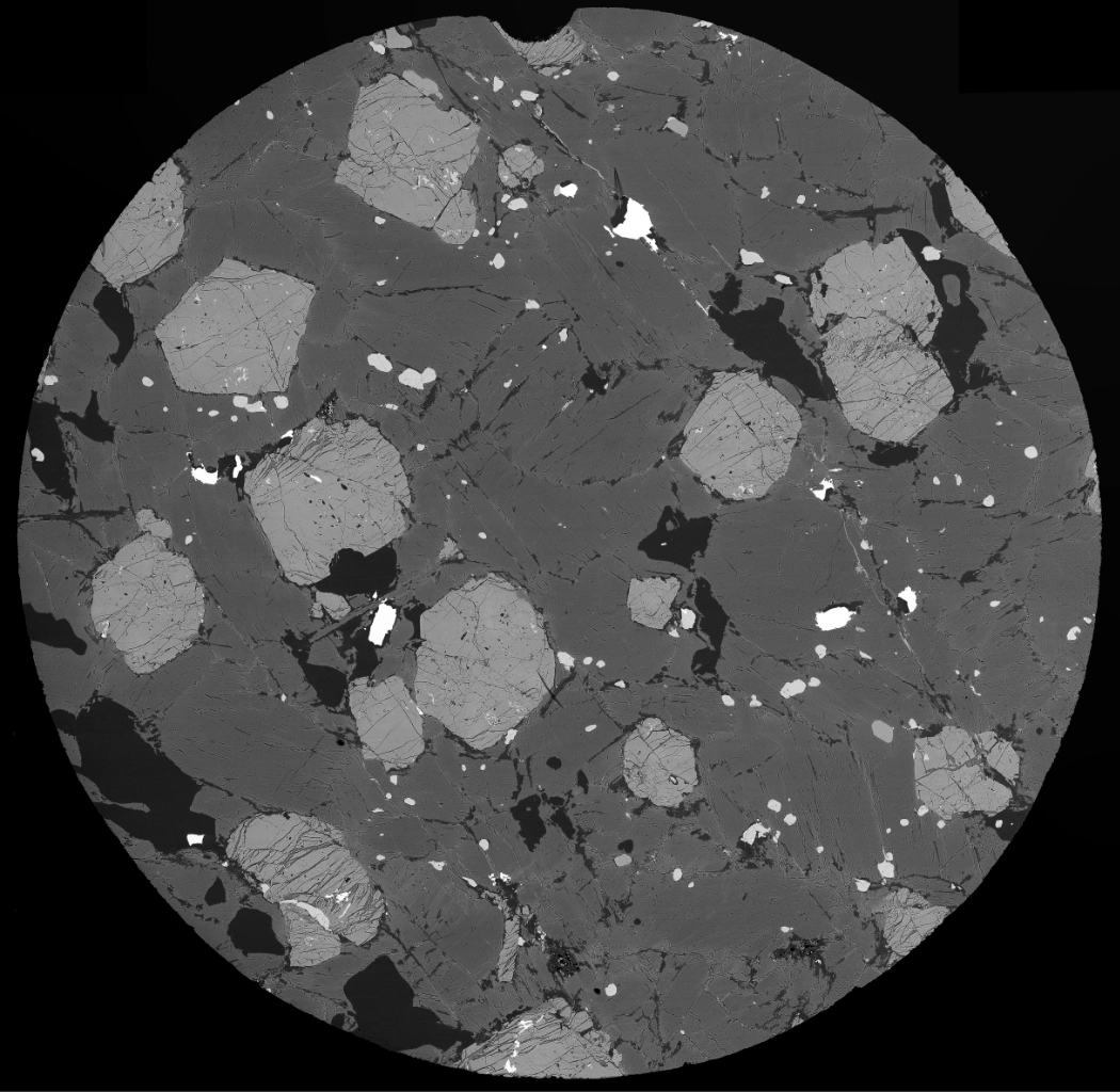 Garnets in silicate matrix · BSE phase contrast
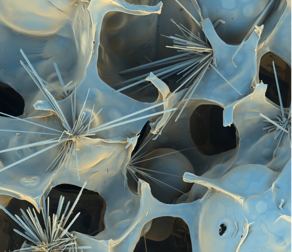
 Framboidal pyrite in sedimentary matrix · BSE
EDS — Energy-Dispersive X-ray Spectroscopy
EDS detects characteristic X-rays emitted when the electron beam ionizes inner electron shells. Each element emits X-rays at specific energies — a chemical fingerprint. By measuring those energies and intensities, the SEM identifies which elements are present and maps their spatial distribution.
EDS provides spectra (energy vs. counts), elemental maps, point analyses, and compositional line scans. Spatial resolution is limited by the X-ray generation volume, typically in the micrometer range for bulk samples.
▸ Technical parameters & Moseley's law
The energy of characteristic X-rays is linked to atomic number by Moseley's law:
This is why EDS can identify elements — each Z produces a unique set of X-ray energies. Key practical parameters:
- Primary voltage should be ~1.5–3× the critical ionization energy of the line measured
- EDS detector: silicon drift detector (SDD), energy resolution ~125–135 eV FWHM at Mn Kα
- Spatial resolution in bulk: ~0.5–5 μm depending on E₀ and material
- Main limitations: peak overlaps, low-energy absorption, matrix effects, quantification uncertainty
- Carbon coating preferred over Au/Pd for quantitative EDS
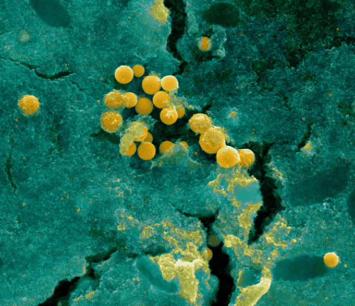
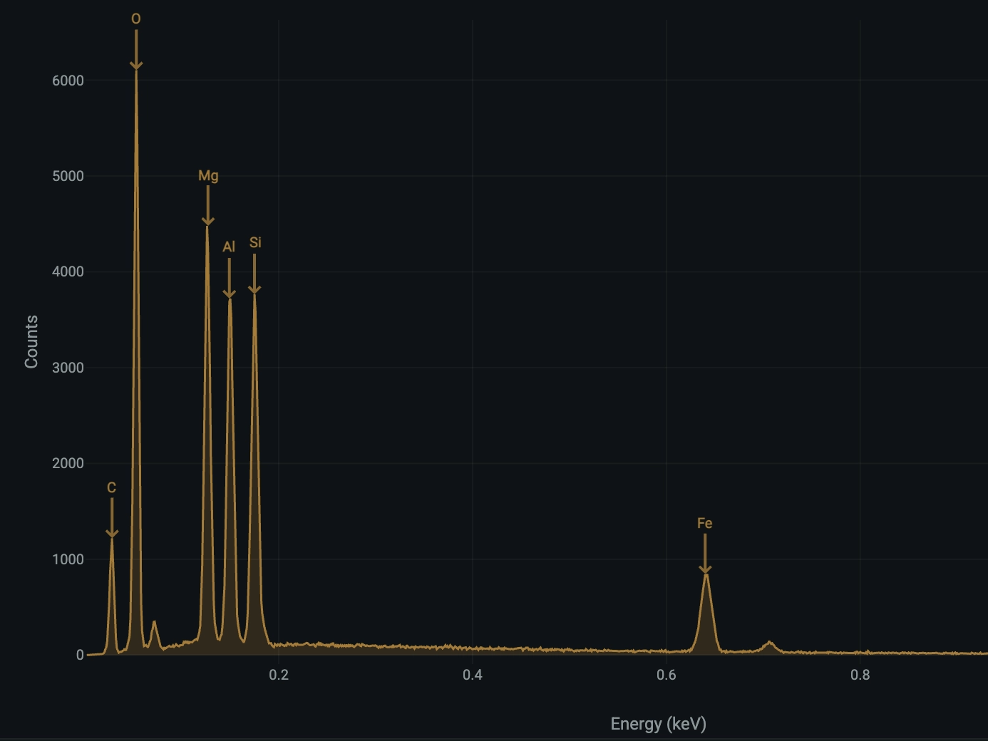
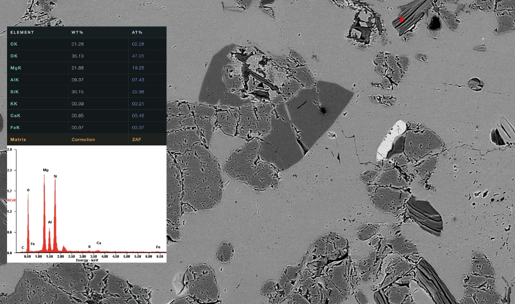 Elemental composition · phyllosilicate · EDS
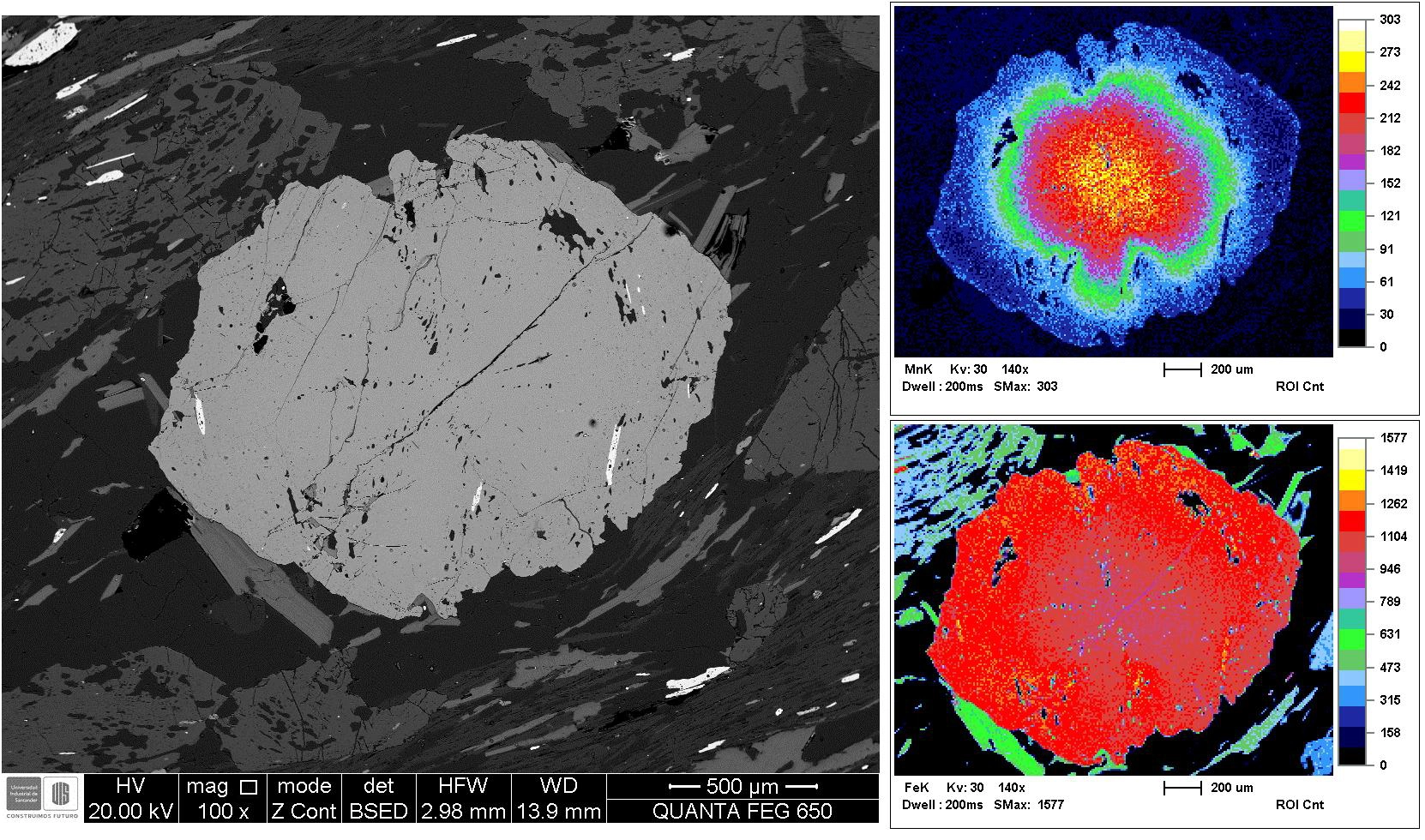 Garnet · BSE + EDS compositional map
STEM-in-SEM — Transmission Mode
Some SEM instruments can operate in a transmission mode when the sample is very thin (<100–200 nm). Detectors placed below the sample collect electrons that pass through it. This mode — STEM-in-SEM — can reveal internal nanoscale structure and provides improved spatial resolution for EDS analysis compared to bulk conditions.
STEM-in-SEM is particularly useful for nanoparticles, thin films, biological ultrathin sections, and laminar material cross-sections prepared by FIB or ultramicrotomy.
▸ Technical parameters
- Sample thickness requirement: typically < 100–200 nm
- Detectors: bright-field (BF) and dark-field (DF) below the sample stage
- Lateral interaction volume is dramatically reduced vs. bulk SEM
- EDS spatial resolution in thin lamella can approach ~5–20 nm
- Useful for: nanoparticles on membranes, FIB lamellae, cryo-sections, thin membranes
- Not equivalent to dedicated TEM/STEM, but accessible without a full TEM instrument
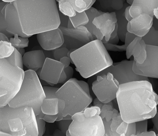
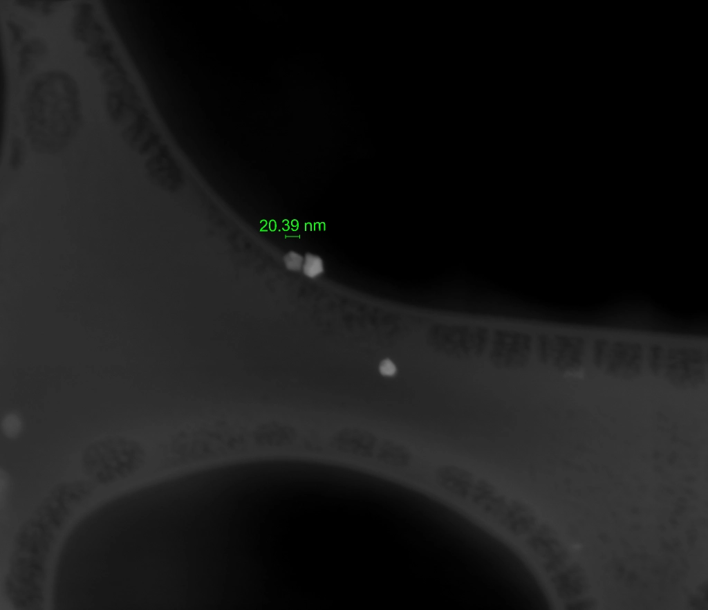 Ti nanoparticles · STEM-in-SEM mode